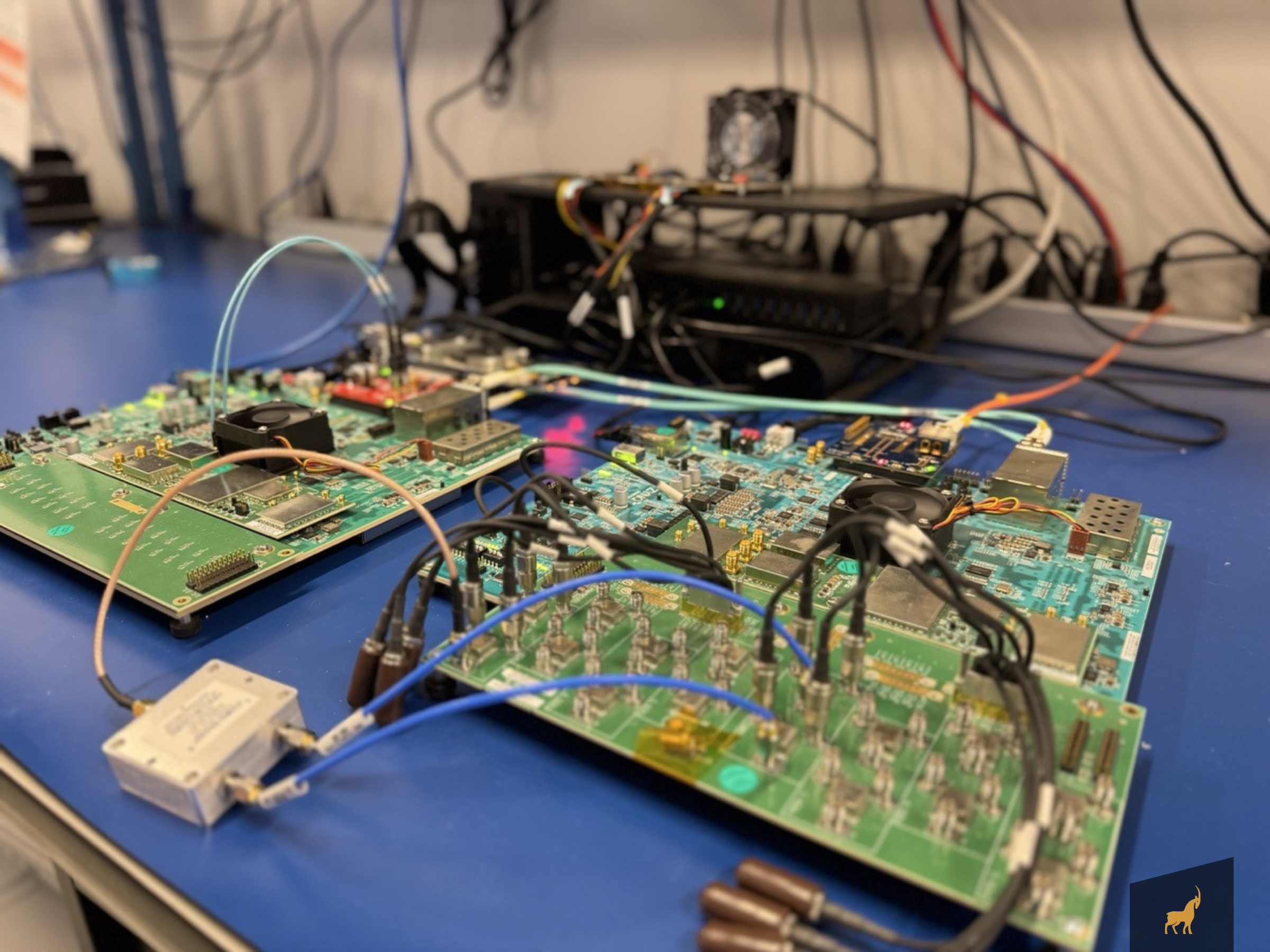
In this post, I want to focus on Field-Programmable Gate Arrays (FPGAs), how Capella Space utilizes them, and the team behind our complex FPGA designs.
In my experience, FPGAs are often overlooked despite their enormous flexibility. When using FPGAs, you’re effectively configuring your own digital logic—registers, Look-Up Tables (LUTs), RAM blocks, and many hard IP cores (DSP, networking, data storage, etc.)—all connected through switch matrices and routes. This flexibility comes at the cost of high-power consumption and design complexity. Because FPGAs are frequently paired with processors, vendors often place both on the same die, known as a System on Chip (SoC).
At Capella Space, we use FPGAs and SoCs as both the heart (flight computer) and brain (payload processor) of our satellites. The payload processor is responsible for:
- Sending and receiving RADAR pulses
- Compressing RADAR data
- Storing and manipulating large SAR collects
- Downlinking these SAR collects
All these operations occur at a data rate of several gigabytes per second (GB/s), which requires the inherent parallelism of FPGAs. Leveraging the NVMe standard to connect Solid-State Drives (SSDs) in a RAID configuration enables On-Board Processing (OBP), including GPU-based tip-and-cue scenarios.
Our current development uses a hybrid FPGA device called a Radio Frequency System on Chip (RFSoC), which integrates Programmable Logic (PL), high-speed data converters (ADCs and DACs), and a processing system (several ARM cores running Linux). This makes the RFSoC a powerful Software-Defined Radio (SDR) that operates in the gigahertz RF spectrum. Using such a highly integrated device significantly reduces Size, Weight, and Power (SWaP).
When it comes to FPGA innovations, I’m always excited to work with the newest capabilities, such as Network-on-Chip (NoC), updated FFT IP cores, and data converters with extended bandwidth and precision. Typical challenges that accompany FPGA design include:
- Requirements engineering
- Resource utilization
- Internal (AXI) and external memory interfaces
- Placement and timing constraints
- Clock Domain Crossing (CDC)
- Timing closure
- Validation, verification, and testing
- For SoCs: PS-PL interfaces and OS considerations
- For high-radiation environments: radiation mitigation
The success and quality of FPGA designs are tightly coupled to the design tools that synthesize and implement hundreds of thousands of LUTs, thousands of multipliers, and hundreds of megabits of memory. Typically, the design process is centered around graphical design entry (which can also be scripted), with a focus on processor system configuration and connectivity through block design. The block design incorporates Hardware Description Language (HDL) modules directly or routes to external HDL modules. When needed, methods such as partial dynamic reconfiguration and high-level synthesis can be applied.
To make our FPGA builds reproducible and expose bugs early, we use a containerized Continuous Integration (CI) system with unit tests. This CI pipeline triggers the OS build pipeline on tagged builds to generate an SoC image—including PL bit files, PS configuration, Linux kernel, and software applications.
Earlier in my career, I worked on a system (CMS at the LHC) that interconnected hundreds of FPGAs via multigigabit transceivers, resulting in extreme parallel computing performance. In addition to this scalability, HLS played a key role in implementing the physics algorithms required for the particle accelerator.
Radiation mitigation for FPGAs is particularly challenging because high-energy particles can corrupt not only your data but the hardware configuration itself. A single particle can flip a bit in the FPGA’s configuration RAM—turning, for example, an AND gate into an OR gate. To make matters worse, the peak directional proton flux of the sun (in a 5-minute integral) can fluctuate by five orders of magnitude. Designing for worst-case conditions can mean preparing for rare but mission-critical events. Engineers may adaptively mitigate radiation effects to reduce the redundancy overhead.
To tackle the challenges inherent in developing the advanced FPGA designs needed for cutting-edge SAR, I’m grateful to work with a very talented and experienced team distributed across the U.S. I’ve recently had the opportunity to grow the team with more junior engineers, and the collaborative knowledge-sharing culture has been invaluable.
I work best when I’m contributing beyond code reviews—experiencing technical pain points firsthand and staying current with FPGA and SoC technology. That makes me a working manager, and while the hands-on technical work is energizing, it needs to be balanced to effectively support the team. In terms of leadership style, I prefer macro-management wherever possible, empowering team members through trust, shared decision-making, and a positive, inclusive environment.
In summary, FPGAs and SoCs excel when a project demands low latency, precise timing, and parallel computation—essentially allowing you to configure your own hardware. They can be used for everything from prototyping the next generation of CPUs to building a full telecommunications modem or a spectrum analyzer. At Capella Space, we rely on FPGAs and SoCs as our flight computers and payload processors for compressing, storing, manipulating, and downlinking SAR data.
With Capella Space now joining IonQ, we’re excited to connect with more FPGA developers and help bring quantum sensing and quantum networking into space. FPGAs are ideally suited for the picosecond- to nanosecond-level timing precision required for quantum-enabled systems.